In universities worldwide, students are discovering the transformative power of simulation and mastering its applications to tackle diverse challenges across industries. Simulation-based learning brings reality closer to the classroom, transforming the educational landscape and enhancing students' engagement with real-world scenarios.
Universities are expanding their engineering curricula to keep up with the ever-evolving world of modern engineering. Training future engineers in simulation is increasingly recognized as a vital component of professional development.
IMT Elevates Engineering Education
Mauá Institute of Technology (IMT) is a private, non-profit institute in São Paulo, Brazil, that gives engineering students the advantage of learning how to use simulation throughout their chosen program. IMT has provided students with leading educational opportunities in business management, design, and engineering for over 60 years. Its engineering department boasts nine different programs that range from food engineering to mechanical engineering. Students gain plenty of experience in using Ansys simulation tools thanks to support from the Ansys Academic Program and Ansys Apex Channel Partner ESSS.
Simulation Meets the Classroom
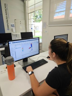
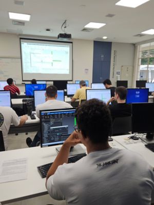
IMT engineering programs are five years long and offer many opportunities for extracurricular courses and disciplines. With an Ansys Academic Multiphysics Campus-Wide Solution, the university has comprehensive access to Ansys simulation tools, enabling the integration of simulation across its engineering curriculum. In their second year, students traditionally have their first experience with Ansys simulation, beginning with Ansys Granta EduPack teaching software for materials education. Throughout the program, students add to their simulation skills with exposure to Ansys tools embedded into each engineering track.
Students gain years of experience in Ansys tools such as Ansys Fluent fluid simulation software, Ansys CFX computational fluid dynamics software, Granta EduPack software, and Ansys Mechanical structural finite element analysis software before they even enter the workforce. They are given opportunities to simulate challenges ranging from understanding the aerodynamics of airplanes and race cars to assessing the risk of brain aneurysms. In fact, simulation is such a highly requested and attractive feature of the program that IMT is now offering it as a “special project and activity” available to first-year students, and an elective discipline for senior students comprising a broader use of simulation in mechanical engineering.
Learning Through Numerical Simulation
Courses in programs like the mechanical engineering track are structured to enable students to study real-world phenomena central to industry applications. Students become well-versed in numerical simulation, particularly in mechanical, chemical, civil, and electrical/electronic engineering courses. For example, the mechanical engineering program involves stages that take the students from computer-aided design (CAD) problem modeling to geometry creation, mesh generation, setup, solution, and post-processing. Students complete even further steps of verification and validation when conducting numerical analyses.
“We start to teach numerical simulation in the third year … and as the years pass, we start to increase the difficulty level so they can study more complex problems,” says associate professor and course coordinator Dr. João de Sá Brasil Lima.
Engineering Education from Every Angle
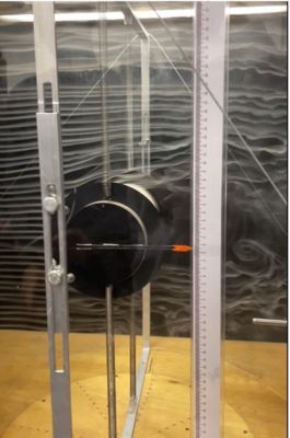
Thanks to the “360ᵒ approach” of IMT’s engineering department, students are gaining a better understanding of physical phenomena through hands-on modeling. Students study a theoretical problem using numerical simulation in both a classroom and laboratory setting, where they can see the problem in real time and focus on its experimental, numerical, and analytical aspects.
“We are not just giving the student an average experience with simulation," explains Dr. Joseph Youssif Saab Jr., energy and fluids professor at IMT. “We believe it really drives the understanding of concepts, which you can use for simulation and then validate with experimental testing. We are making sure students can deeply understand the concepts involved.”

Simulation Sparks Engagement in Students
Undoubtedly, students at all levels of the program strongly favor the focus on simulation. “The students really like to use the tools during classes. They get more enthusiastic to study [phenomena] that previously were only taught on a blackboard,” says Lima. He shares that learning how to use Ansys tools helps capture students' attention, which enables them to better understand each tool's features. This knowledge equips students to understand and apply the appropriate tools when they enter the industry post-graduation, and an increasing number of students are seeing this happen sooner rather than later.
Student Teams
Students at IMT not only benefit from award-winning engineering classes, but also the opportunity to get hands-on experience through numerous student teams.
A well-known opportunity on campus is the MAUÁ Racing Formula SAE team. Formula SAE is an international engineering competition held in Michigan, organized by SAE International, where college students design, build, and compete with small formula-style race cars. The team from IMT took first place in the Engineering Design contest in 2024.
Taking Learning Beyond the Classroom
At IMT, it’s not uncommon to see 95% of graduating engineering students or more completing their programs with a job offer. Drs. Lima and Saab credit the multidisciplinary approach to teaching simulation — particularly numerical simulation — with keeping this employment number so high. Previously, employers would invest a great deal of time in training new employees in computer-aided engineering (CAE). IMT aims to increase the employability of its graduates by teaching them the skills they need to hit the ground running as new employees in any engineering field.
“We have introduced Ansys tools for problem-solving in many disciplines for many years now, and students are being selected by some industries based on this experience, in some cases, which is what we planned,” Dr. Saab says.
One student story in particular will always stick with the engineering staff at IMT: A student who oversaw numerical simulations for the MAUÁ Racing Formula SAE team as an extracurricular project made quite the impression on a new employer when he suggested they incorporate simulation into their workflow. After developing and proving a case for simulation, the employer was convinced that simulation could be the solution to several of their challenges. The student went on to start and run the first simulation department at that company, powered entirely by Ansys tools.
“One thing that really makes us happy is to see our students finish their program, go to companies to work, and still find new problems and situations that can be studied with numerical simulation,” says Dr. Lima.
Integrating Local Industry
IMT is not only sending its graduates out into the industry with an advanced simulation skillset, but it is also bringing the industry to the classroom. Engineering paths may vary, but it’s the shared use of simulation tools and comprehensive education that strengthens the IMT engineering department as a valued partner within the industry in Brazil and beyond. “We are developing partnerships in different ways,” Dr. Saab says.
A chemical plant component manufacturer has joined forces with IMT over the past five years to challenge up-and-coming engineers in a real-world scenario related to one of their products. In the challenge, an engineer from the company presents students every year with the geometry of the company's product. The students are then challenged to optimize the product using simulation, towards some specific final requirements. The engineer visits the class throughout the semester to check students’ progress on completing the challenge, then evaluates the final simulations and awards the team that reached the best results with a certificate signed by the company and IMT.
Another type of interaction happens within the HPA project, where the requirements are developed in-house, but engineers from an aircraft manufacturing company assess the results for each design team twice a year. This invaluable chance to gain hands-on experience and interact with industry professionals is just one example of how IMT raises the bar in simulation education.
Additionally, approximately 40 IMT students participate in the NAE Grand Challenges Scholars Program along with mentor professors from IMT, using Ansys simulation in research projects and beyond.
Pushing Boundaries in Engineering Education
Despite the impressive courses, collaborations, and research projects happening at IMT, the engineering department is always looking to advance the future of the program. Ultimately, the department aims to implement project life cycle management (PLM) into its catalog of existing tools. “If you can replicate the industrial environment inside your school, you can teach the students to go seamlessly into the industry without experiencing many differences,” Dr. Saab says. Professors of engineering at IMT are focused on finding the right solutions to further familiarize students with real-life industry experiences.
IMT continues to advance its role as a leader in engineering education by embedding simulation use into its programs. Just recently, IMT was awarded the highest grade (Grade 5) by the Brazilian Ministry of Education for its mechanical engineering courses. Additionally, IMT also obtained a Grade 5 among all mechanical engineering courses in Brazil (1st place in the Course Concept metric). “We are sure that our teaching in numerical simulation was one of the factors that contributed to these excellent results,” says Dr. Lima. By equipping students with these high-demand skills, the university continues to empower students to solve the complex challenges they will face in their careers.